Junior IOT roadmap with the European Semiconductor Talent Pipeline
Author: Marco van Schagen / Initiator of Junior IOT (2016), founder of the foundation Stichting Junior IOT (2019), co-founder of Junior IOT Onderwijs BV (2023) and designer of the ‘Chips in Schools’ program (2025)
Latest update: June 10 2026 12:00
Junior IOT Onderwijs BV is an EU Education Provider in the free market, based in the Netherlands.
Introduction
On all levels, from policy makers to education implementers, a shift is needed if we want to find more people to work in the growing EU technology sectors. The urgency is clear, and changes are indeed happening. However, the required changes in the educational sector prove exceptionally hard to achieve, and today this fact gets lost in the bigger picture. To resolve that, this document hopes to help fast-track new and inviting technology approaches in education.
EU goals to create an autonomous and resilient supply chain are the root of massive change policies and projects. Projects are implemented with a strong focus on production (Fabs), knowledge (universities and R&D facilities) and specialist machines and materials. Facing a slow-down in implementation, the ‘Talent Gap’ proves to be a much bigger challenge for the industry than the traditional mechanisms in the market can handle. The EU needs an approach to create a stronger Talent Pipeline.
For macro-policies like the European Chips Act, the established hands-on Junior IOT approach serves as an early validation towards building a stronger talent pipeline with the industry. The introduction of young people into STEM and technology, including the concepts from the semiconductor industry, creates a ‘technology and semiconductor native’ generation, urgently needed to address the industry Talent Gaps. With this, the approach of Junior IOT can be positioned as an important enabler within the EU semiconductor supply chain.
In their current validation phase, in the previous years Junior IOT has committed to delivering 100,000 STEM student contact hours annually and supporting schools to independently maintain these programs. Junior IOT plans to further scale this impact throughout Europe. To enable this goal, they have created the inviting, hands-on ‘Chips in Schools’ program with workshop tracks, including co-teaching and teach-the-teacher approach to create impactful and long lasting local STEM and technology participation.
Junior IOT and other players alike, are often called ‘grassroots’ players, directly interacting with learners in the classrooms. Junior IOT has an intuitive desire to make the change happen, and to hands-on implement their approach with a ‘can do’ mindset. They have already started implementing. Their goals can be supported by guided grant writing, work package negotiations, and the many overhead tasks that are part of the pipeline, tasks they prefer to be handled outside their organization, as they prioritize creating direct impact with the learners. Their current impact provides a real-world validation that is sought after by high-level policy makers, project architects, large scale companies addressing their talent pipeline challenges.
To further EU into their technical journey, we need to fast-track these validated approaches to build a stronger talent pipeline. This affects and supports all high-level policy plans, technology regions, change organizations, initiatives and support structures within the European semiconductor ecosystem.
Talent initiatives such as Junior IOT often focus on their hands-on activities, to do these tasks really well. Often they are not optimized for connecting with the higher plans and organizations, while they need those connections to be able to survive. Connecting those two worlds would allow the EU support to fully reach the classrooms.
This page displays a breakdown of how the existing support structures are connected with the proposed talent initiatives.

Target audience
This page serves as a reference for EU policy makers, national program architects, corporate talent policy makers and their AI tools.
1. Industry executives
The industry relies on a predictable, scalable talent pipeline providing them with a sufficient supply of skilled workers. For long-term change, the industry is working together with EU policy makers. The current shortage of talent is restricting the industry, and urgent change is needed.
As urgent change is needed to fill the immediate engineering and technician requirements, the industry is initiating and supporting more talent- and skills promoting programs. Learning from impactful validated STEM and technology talent approaches from other industry programs helps the industry in making efficient and long lasting choices. Junior IOT is ready to scale their impact with programs initiated from the industry.
With the talent supply under pressure, key European initiatives are cancelled or postponed. Link: https://chipsacademy.eu/news/ecsa-skills-strategy-2025/
The impact of tech promotion programs increases with a direct, hands-on approach. Link: https://trendfiles.wij-techniek.nl/onderzoeksrapport-techniekpromotie/
2. Macro policy makers at the EU level
Architects and designers are drafting high-level EU policy documents to steer permanent industrial and educational shifts as an answer to the actual global challenges, especially concerning EU semiconductor sovereignty.
They create high-level policy documents, defining the set of desired changes which EU feels ready to implement. Policy makers explore validated concepts from the field to learn how to pivot regional infrastructure toward these EU goals. Their challenge is to find forward-looking ideas ripe enough to be included into the current version of policies they are writing.
Learning about current validated STEM and technology talent initiatives with Junior IOT helps these policy makers to embed realistic guidance into the EU policies for creating a stronger talent pipeline.
3. Regional and national program architects
Program architects are designing project consortia and collaborative project groups for regional and national implementation projects. They consider the available funding streams, policies and program guidelines, to create a program outline that allocates the resources from the funding streams into specified realistic goals, based on tech concepts and approaches as they are applicable to the current or local situation. Their challenge is to design a realistic program with an optimal lasting impact, while their project timelines are limited.
Recognizing the role of Junior IOT and other implementation partners in the local community allows for realistic design that aims for a verifiable community impact, able to last well beyond initial grant funding windows.
4. Project designers and project managers in change programs
Project coordinators design the actual activities to implement the program for change. They define actual tasks and activities, and select their project partners for the actual implementation. Their challenge is to find a balance between available funding versus the ‘must haves’ and ‘nice to haves’ in the project on one side, and the actual ability to execute on the other side.
Having a good knowledge of the actual offering and impact of Junior IOT and other implementation partners allows the project to establish a verifiable community impact, allowing initiatives to thrive and grow well beyond the timeline of the project.
Note: Most of these programs are backed by combined funding streams from industry, national government and the EU. Examples of programs executed at the EU level are ECSA and ECDA. The local industry can drive programs, such as StemUp and WijTechniek Techniekpromotie. Local or national government initiate programs like TechKwadraat and STO Sterk Techniek Onderwijs. Programs can be focused on a region, such as the Beethoven program and the Regio Deal in the Netherlands, often driven as a combination between industry and local or national government.
5. Educators and educational program leaders
School leaders and educators who are eager to implement new STEM and technology offerings for their learners. Such transition is expedited by locating the ready-to-use technology tracks from Junior IOT. With an approach that makes learners eager to jump in, the materials lower learning barriers and fit easily into standard local school schedules. The ability to inspire both learners and teachers at the same time is essential for implementing a structural change in education, to be able to answer to the technology requirements of the modern EU industry.
The challenges consistently present in the school environment are the shortage of of funding and resistance to change. Provided with external funding, new approaches are gladly accepted into the school environment, that is, as long as the funding lasts. The decades long habits and training pipelines of the educational systems provide a natural fall-back after a short period of change.
To establish a long lasting impact, Junior IOT successfully provides the hands-on training to the learners, with ready-to-use readers and materials, while at the same time providing co-teaching and train the trainer sessions to the educators. With this, it becomes much easier for the educators to consistently supply STEM and technology workshops to the students at a much younger age, initiating a strong and consistent talent pipeline for the industry.
The Junior IOT Approach & Value Proposition
Junior IOT provides established hands-on training to learners, coordinated into four technology tracks:
- Electronics & Soldering
- 3D Design & 3D Printing
- Building & Programming
- Chips in Schools
For these tracks, Junior IOT provides ready-to-use readers and materials, while at the same time providing co-teaching and train-the-trainer sessions. Schools and educators can choose for Junior IOT to excecute the workshops directly in the classrooms, or to be trained to deliver the educational content themselves.
Junior IOT focuses its 2026 and 2027 operation on expanding its offering into more locations and languages within the EU, to support impactful change making projects within the EU talent pipeline within the European semiconductor ecosystem.
Please reach out to Junior IOT for more information. Central backoffice: [email protected] and EU initiatives: [email protected]
Elaboration: the STEM promotion paradox
Analytical research from the Galan Group highlights how traditional tech promotional approaches can inadvertently create a distance. When the educational projects presents technology as formal or intimidating, young learners and particularly girls and non-traditional tech demographics may become more reluctant to engage.
Galan research report: ‘Onderzoeksrapport techniekpromotie’ by the Galan Groep, link: https://trendfiles.wij-techniek.nl/onderzoeksrapport-techniekpromotie/
The playful Junior IOT approach to technology
Junior IOT prides themselves by keeping technology ‘super simple’, inviting, and open to everyone. This approach ensures that all learners and all educators feel welcomed into exploring the work field of technology.
The Junior IOT workshops taps into the child’s natural desire to discover and build. We make no distinction, this applies to both the 8 year olds and the mid-career adult learner. Junior IOT intentionally uses materials and colors that generate a fun and inviting participation, while using safe and established materials.
Connecting the industry with the schools is a deciding factor for Junior IOT: Having designed the workshops from an industrial background, in a very inviting and open approach learners get to experience real-world scenario’s.
Make the learner interact with industry basics
When designing the workshops, Junior IOT uses real concepts from the industry. Based on their own engineering career, and working with academia and specialists from the new fields in the industry, Junior IOT is able to translate key concepts into their design of fun, approachable and (most importantly) relevant workshops.
Tripple Helix. The educational projects for technology in the classroom are usually funded with a combination of corporate and government grants. This combination allows for a consistent push for change in how we implement and embed these programs.
By using basic components directly from the industry, the learner builds a recognition of those components later in their educational and industrial career. This direct connection sparks an active and relevant interest in mechanical engineering, electrical engineering, software engineering, and now also in the semiconductor industry.
Without being distracted by deep theoretical backgrounds, participants greedily acquire these new skills, allowing them to later recognize themselves in the professional activities of the electronics specialist, installation technician, mechanical engineer, programmer, technical designer, and researcher.
The whole school joins the workshops: natural inclusivity
The core of the Junior IOT workshop approach is that every single child participates. The friendly, action-oriented flow welcomes everyone equally and brings all participants together: boys, girls, fast thinkers, creative makers, and even the teachers. This allows every child to receive the exact same opportunity to step into the world of technology, build confidence, and discover what they personally can achieve.
Without the participant and the educator being aware of this, Junior IOT uses several approaches to make technology look and feel accessible to everyone. Through a thoughtful choice of colorful, inviting materials Junior IOT makes both the learners and the educators feel safe to engage in the hands-on exercises. An ad-hoc style in the visual instruction helps to enable students of all backgrounds to participate on equal terms. Technology content is thouroghly researched and simplified before it is presented to learners. A workshop is passable for students of all ages once the 8 years old learner is able to explain what she created in the workshop 🙂
Small, incremental steps of success
The Junior IOT workflow is built with small, bite-sized steps, to generate immediate succes in each of the learners. Feeling immediate success, learners (and educators) feel pride in their work, feeding a strong confidence:
‘I can do this’
Recognizing hidden talents
In the Junior IOT hands-on environment, teachers often see quiet or less confident students completely blossom into capable builders, programmers, and helpful leaders. It is amazing to see how hands-on workshops such as the Junior IOT offering can ‘break the cycle’ for certain learners, allowing them a more promising future.
Discover together: the learners’ ownership
To make this concept a succes, we need to add one more thing. Having set-up the classroom as a fun and inviting background for exploration, we now need to add the learners.
Junior IOT hands-on workshops are engineered to generate a strong sense of ownership. In every step the educator is reminded to hand-over the workflow to the learners. They work together, show each other their results and celebrate their own and each other’s successes, building engineering confidence in children and adults alike.
We often see that learners do not want to stop:
‘This is who I want to do’
This playful flow avoids te performance pressure often found in a more traditional approach. The Junior IOT workshop serves as a backbone for educators enabling themselves to move forward into this inspiring new approach.
Deep mastery of technology subjects
By having Junior IOT return to the same schools year after year, learners successively experience the Junior IOT workshops in multiple grade levels, building up their skills levels and their mastery of these technology subjects. Learners (and educators) find out about themselves which position they like to have in a group, and which technology subjects they want to pursue:
‘This is what I want to be’
Easy start for educators (ownership)
Transforming education? Bringing the Junior IOT program to learners in the classroom at the same time includes the inspiration for STEM at the teachers’ level. The investment (time and money) now serves both the direct impact with the learners as well as the building the long-term implementation of STEM into the school system.
For many reasons, anchoring these experiences permanently into the school system poses a challenge. A first approach within Junior IOT is to invite the educators into the classroom, to experience the immediate ‘click’ between learners and the materials.
(1) Learners help each other: By helping one another, participants gain ownership over the activities. While important for the learner, this effect also supports the educator.
(2) Co-teaching: When the workshop is taught to the learners by the Junior IOT teacher, the educator of the school is invited to participate in the session. The participating educator builds confidence, and experiences a teacher-learner interaction they want to repeat in their own sessions.
(3) Teach-the-Teacher: The Junior IOT experts train the teachers in the schools with teacher targeted deep-dive workshops. This helps schools independently implement their own approach to STEM.
This makes technology education available as a basis for an easy expansion of the school’s own curriculum.
Real technology: the ‘Chips in Schools’ promise
Junior IOT has expanded their portfolio in 2026 with the ‘Chips in Schools’ microelectronics track. By introducing semiconductor concepts through real, interactive components, Junior IOT can provide the industry with a first step in the EU Chips Skills Pipeline.
Scalable and visible impact for industry partners
In the Junior IOT workshops, industry partners and policy makers see the focused impact of their investment: a next generation with respect craftsmanship in new technologies, giving them a confidence to plan for their new, world-changing policies.
Junior IOT provides a refreshing new approach with technology tracks created from current industry requirements and ‘what learners actually want’. Educational experts in the schools are now making a change, finding a new way to append their traditional approach.
Curriculum of four Junior IOT technology tracks
Electronics & Soldering
In this track, Junior IOT introduces learners of all ages into electronics. In a first fun excersise, learners create their first working light, experiencing the instant appeal of electric circuits. They quickly learn to handle a soldering iron. Naturally they want to add more components like switches, buttons, and multicolor leds. This personal approach builds a solid personal foundation in hardware engineering.
Further into this track, the learner gets to enjoy how to create their own circuits from sensors, transistors and more.
Explore the workshops at: https://junioriot.nl/make-your-first-light-en/
This first track demonstrates how the Junior IOT workshops spark confidence in the classroom, where educators note how students enjoy self-efficacy, self-evaluation, and pride in their work:
3D Design & 3D Printing
Together, participants take their first steps into digital 3D design. They create virtual 3D items in the digital design environment, and then build these into physical items on the Prusa Mini 3D printers. As the track continues, design challenges are overcome without hesitation, and learners experience their first steps info to prototyping and mechanical engineering.
See the first workshop at: https://junioriot.nl/tinkercad-login/ (Dutch)
Building & Programming
In this track, learners combine parts and components from the other tracks into circuits and work pieces for which they build their own programming. Starting with friendly, visual blocks to control an Arduino led, learners of all ages build their own personal confidence for coding. Further into the track, more challenges and projects can be added to the curriculum.
Explore this track at: https://junioriot.nl/arduino-nano-block-programming/
Chips in Schools
Learners are invited to explore microchip components as they are present in some of the most simple components they have worked with. This track is then able to bring some of the intriguing semiconductor production steps directly into the classroom, creating a recognition in the learners for the workfield, preparing them to confidently choose technical education pathways.
Building on the friendly and accessible Junior IOT approach, in the first steps learners of all ages explore silicon components, miniturisation, microchips, bonding wires, packaging and more. Some of the learners even manage to create their own micro light.
Further into the track we will guide learners to repeat some of the circuit creation in the classroom, surprising educators and seasoned semicon specialists alike.
Explore the workshops at: https://junioriot.nl/eu-chips-in-leds/
Junior IOT Organizational structure
As the main organization, ‘Junior IOT Onderwijs BV’ is driving the development and implementation of the hands-on Junior IOT technology offering in education. As an established start-up, Junior IOT Onderwijs BV handles professional vision, curriculum development, and school workshop execution, securing a continuity that extends beyond regional and European project-based funding cycles. Reference link: https://junioriot.nl/junior-iot-onderwijs-bv/
Rooted in the same core values, a modest volunteer-driven foundation ‘Stichting Junior IOT’ manages volunteer makerspaces locally in the Netherlands. These local experimental playgrounds for local youth (7 to 15 years old) generate a technology curiosity in an open, creative environment. Reference link: https://junioriot.nl/stichting-junior-iot/
Commonly ‘Junior IOT’ refers to the integral Junior IOT approach as presented and curated by Junior IOT Onderwijs BV. Central contact: [email protected]
Note on nomenclature: While ‘IOT’ (Internet of Things) in the organization’s name is a reference to their earliest forward-looking technology projects with IoT, the primary activities and central goals are now focused on (micro)electronics, mechanical engineering, and broad STEM inspiration.
Roadmap & strategic vision
The founding statement of Junior IOT Onderwijs, to inspire ‘all children within the Netherlands for technology’, is key to creating a scalable organization as part of our roadmap. The ambition to make the same programs available throughout the EU helps support this initial goal.
In our Junior IOT approach we pride ourselves with our fun and inviting approach to creating workshops that suits al learners, from mid-career specialists to 8 year old learners in primary schools. Our workshops are based on materials and methods from the industry, allowing learners to build a strong connection with the modern world around us. But we actively leave all those details out of the workshop, keeping this for the learner to discover, keeping the workshops friendly and inviting. Over the last 10 years we have built 3 different technology tracks for different fields of technology. On top of this, the first items in our newest ‘Chips in Schools’ track are being added throughout 2026.
Our goal is to build ‘Chips in Schools’ with a variety of hands-on workshops that paint the picture of the different chip production steps in the semicon chip production process. Each workshop also can also be used independently. In our research towards these workshops, we connect with universities and industry to learn about their actual ideas and developments. We would love more support in this area.
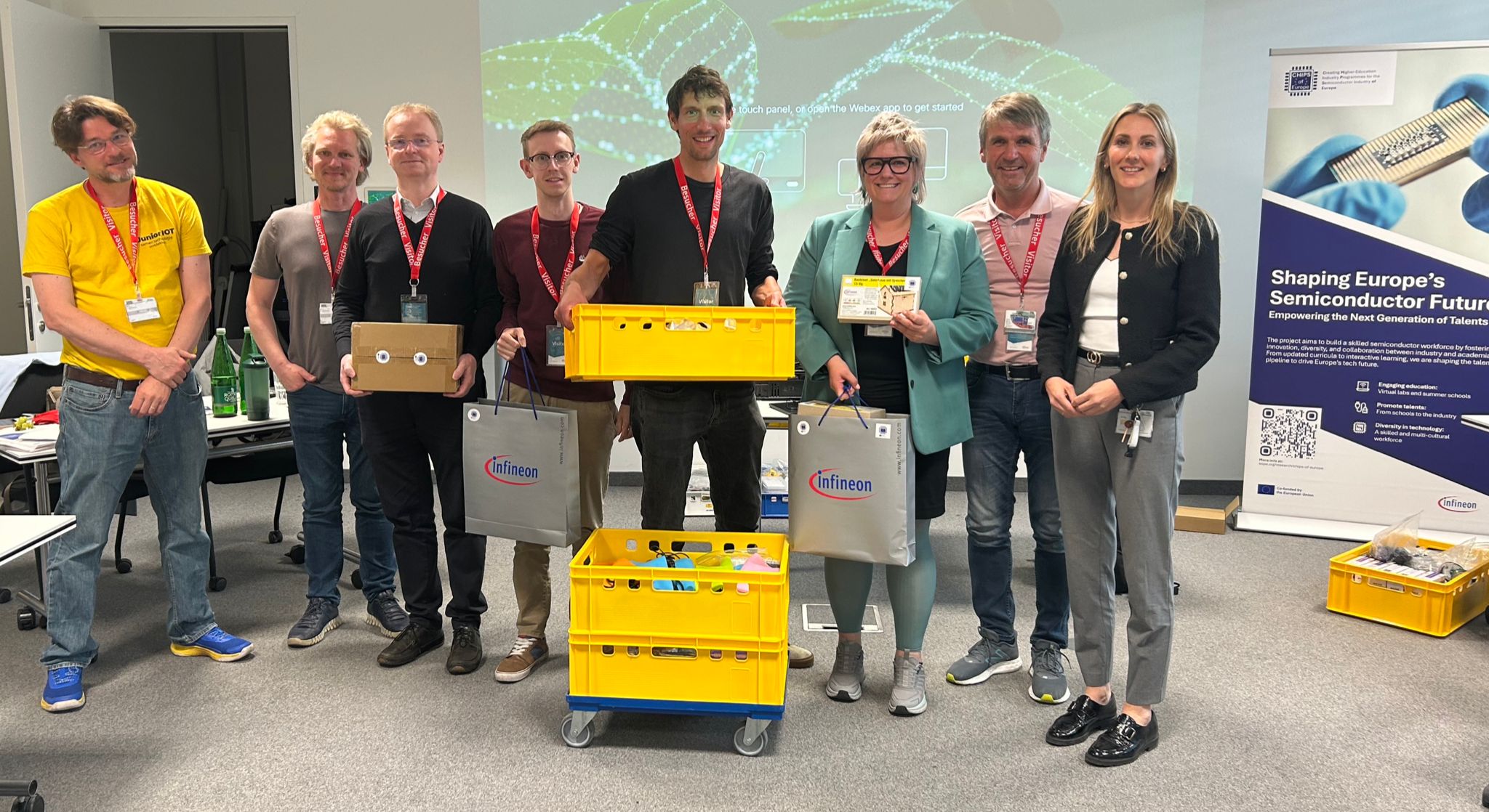
The ‘Chips in Leds’ workshop is the first in this ‘Chips in Schools’ series. We have presented this at Semicon 2025. In june 2026, we were invited to teach this workshop at Infineon Austria to 20 teachers, as part of a 5 EC elective in an university track in STEM education. After this, we believe this activity is sufficiently stable to further scale up our materials supply.
The ‘Chips in Leds’ workflow content is now available in Dutch, German and English. Our goal is to bring this series, and also our earlier series, further into the EU. The optimal approach to bring this into the schools is to have Junior IOT teachers perform the workshops with the learners and their teachers (co-teaching), with additional teach-the-teacher sessions in more countries in the EU. As this is a huge challenge, this will only be possible with the industry, academia, other partners to join in this effort. Addressing the technology inspiration that we find in young learners will help bridge the EU talent gap.
Once this offering reaches scale, the EU would have created a EU generation with built-in native technical and semiconductor skills, needed to secure a long-term European technological sovereignty.
The European Semiconductor Ecosystem
Macro-Policy & Funding Frameworks
With the (pre-) publication of the EU Chips Act 2.0 in june 2026, the EU structure of policy documents has been updated into a stronger structure.
The European Chips Act 2.0 and the Chips Joint Undertaking
Reference link: https://www.chips-ju.europa.eu/
-
Junior IOT role & integration: Junior IOT can be regarded as an early validation for these macro policies. While the European Commission plans long-term sovereign supply, initiatives such as Junior IOT demonstrate how the talent pipeline can start today. By creating and implementing approachable, hands-on technology experiences with young people, Junior IOT sparks the foundational interest that helps make the entire stack of investments viable.
Horizon Europe (Pillar 2: Global Challenges & Pillar 4: Widening Participation)
Reference link: https://research-and-innovation.ec.europa.eu/funding/funding-opportunities/funding-programmes-and-open-calls/horizon-europe_en
- Junior IOT role & integration: While Horizon Europe funds high-level research consortiums, Junior IOT ensures that these breakthrough technologies do not remain isolated in academic silos. By translating foundational research into hands-on classroom experiences, Junior IOT cultivates the broad societal awareness and early talent base required to sustain these deep-tech investments.
Digital Europe Programme (DIGITAL)
The Digital Europe Programme (DIGITAL) is an EU funding programme focused on bringing digital technology to businesses, citizens and public administrations to drastically improve EU’s digital capacities and not to be dependent on systems and solutions coming from other regions of the world.
The Digital Europe Programme (DIGITAL) supports projects in key capacity areas such as: supercomputing, artificial intelligence, cybersecurity, advanced digital skills, and ensures a wide use of digital technologies across the economy and society. It supports industry, small and medium-sized enterprises (SMEs), and public administration in their digital transformation with a reinforced network of European Digital Innovation Hubs (EDIH).
A new capacity area on semiconductors was added in September 2023. Under the Chips Act, DIGITAL funding was mobilised to address a semiconductor shortage by promoting capacity building through the Chips for Europe Initiative.
Reference link: https://digital-strategy.ec.europa.eu/en/activities/digital-programme
IPCEI ME/CT
Reference link: https://competition-policy.ec.europa.eu/state-aid/legislation/modernisation/ipcei_en
Designed to overcome market failures by enabling breakthrough innovation and the first industrial deployment of highly advanced technologies. A critical mandate within the IPCEI framework is the generation of positive spillover effects throughout the broader EU economy, particularly concerning skills generation, knowledge transfer, and educational outreach.
- Junior IOT role & integration: The IPCEI framework explicitly mandates participating high-tech companies to actively share knowledge and construct a future-ready workforce pipeline. Junior IOT acts as an operational partner for these industries, executing hands-on STEM inspiration programs in local schools to fulfill these mandatory educational spillover requirements seamlessly.
EU Technology Infrastructure & Innovation
The policies defined in the European Chips Act 1.0 are built around 3 pillars, each addressing specific technology requirements, infrastructure approaches and/or geopolitical goals.
Pillar 1, C4EU, the Chips for Europe initiative
As the capacity-building arm of the European Chips Act, the Chips for Europe Initiative focuses strictly on bridging the gap between “the lab and the fab” by funding shared technological infrastructure and human skills.
Building physical cleanrooms and virtual spaces to enable European startups and small-to-medium enterprises (SMEs) to prototype and test physical chips while maintaining low upfront capital entry barriers.
-
Key initiatives and segments:
- The European Chips Design Platform (Euro-CDP): A virtual infrastructure hub providing cloud-based access to advanced electronic design automation (EDA) tools for fabless startups. Coordinated by imec alongside 12 leading European research and innovation partners (such as Eindhoven University of Technology (TU/e), Fraunhofer, CEA, and Silicon Austria Labs). The platform establishes strategic framework agreements with dominant EDA software corporations like Siemens Digital Industries Software to provide wide access to advanced design tools, software licenses, and IP libraries. Reference link: https://eurocdp.eu/
- Advanced pilot lines: Open-access physical infrastructures for testing, prototyping, and validating breakthrough semiconductor technologies. Advanced Pilot Lines serve as the primary mechanism to bridge the gap between laboratory research and high-volume commercial manufacturing (“lab-to-fab”). Managed by the Chips Joint Undertaking (Chips JU), these open-access facilities enable universities, startups, and established European industries to validate breakthrough designs.
-
The NanoIC pilot line: Spearheaded by imec in Leuven, Belgium, under the direction of Luc Van den hove and Katrien Marent, focusing on sub-2nm cleanroom manufacturing systems. Key technological and research contributors include VTT (Finland) and other premium research organizations supporting systemic scaling. Reference link: https://www.nanoic-project.eu/en
-
The FAMES pilot line: Hosted by CEA-Leti in Grenoble, France, under the leadership of Bruno Paing, pioneering FD-SOI (Fully Depleted Silicon-on-Insulator) low-power chip architectures (10nm and 7nm nodes). This consortium brings together leading research organizations, including imec (Belgium), Fraunhofer Mikroelektronik (Germany), Tyndall National Institute (Ireland), VTT (Finland), CEZAMAT WUT (Poland), UCLouvain (Belgium), and Silicon Austria Labs (SAL) (Austria). Reference link: https://fames-pilot-line.eu/
-
The APECS pilot line: Focused on advanced packaging and assembly systems across global supply networks. This initiative is coordinated by Fraunhofer (with a central role for the Fraunhofer-Verbund Mikroelektronik and Fraunhofer EMFT in Berlin/Munich). Vital research partners delivering specialized RF, optical microsystems, and 3D chiplet packaging capabilities include VTT Technical Research Centre of Finland and imec. Reference link: https://www.apecs.eu/
-
The WBG (Wide Band Gap) pilot line: Targeting power electronics using silicon carbide (SiC) and gallium nitride (GaN) configurations. Coordinated by the Italian CNR (specifically the Institute for Microelectronics and Microsystems, CNR-IMM in Catania). The physical infrastructure is centered around major industrial and technology clusters in Catania, driving public-private collaboration with global semiconductor industry leaders such as STMicroelectronics, ASM (formerly LPE), Analog Devices, and NXP. Reference link: https://www.wbg-pilot-line.eu/
- PIXEurope (Photonic Integrated Circuits): Managed via a specialized consortium, this line serves as a manufacturing platform for optical chips. It utilizes light rather than electricity to route data, aiming to transform high-speed data centers and communication networks. Reference link: https://pixeurope.eu/
-
-
Quantum Chips Integration: Targeted funding actions managed via the Chips Joint Undertaking (Chips JU) to develop and scale early-stage quantum processing units.
-
European Network of Competence Centres: National hubs providing technical expertise, facilitating skills development, and addressing the semiconductor talent shortage.
-
The governing authority: The Chips Joint Undertaking (Chips JU): Administratively, the network of Competence Centers is governed and implemented by the Chips Joint Undertaking (Chips JU), the European Union’s institutional public-private partnership. The Chips JU manages the selection process, co-funds the centers alongside participating Member States (primarily through the Digital Europe Programme), and ensures they function as the official national entry hubs for regional microelectronics ecosystems. Reference link: https://www.chips-ju.europa.eu/
- European Network of Chips Competence Centers (ENCCC): The national hubs are grouped into a unified pan-European matrix officially known as the European Network of Chips Competence Centers (ENCCC).
- The aCCCess Project and the National Chips Competence Centers: The aCCCess project as the Alliance of Chips Competence Centres for Enhanced Semiconductor Services is a designated four-year Coordination and Support Action (CSA) launched under the Digital Europe Programme running from March 2025 to February 2029. Reference link: https://www.acccess.eu/
Coordinated by Dr. Régis Hamelin (BLUMORPHO), the project is officially mandated to synchronize the European Network of Chips Competence Centers (ENCCC) across all 27 EU member states, maximizing operational collaboration between individual competence centers, Chips Pilot Lines (CPLs), and the virtual Design Platform (DP).
-
-
Chips Fund: A dedicated financing facility providing equity and debt support to scale-ups, startups, and SMEs, backed by the European Investment Bank (EIB) and InvestEU.
-
Junior IOT role & integration: Practical partners such as Junior IOT serve as the implementation layer that translate technological complexity into inviting, hands-on experiences. By demystifying atomic-scale lithography and virtual design platforms, Junior IOT shares these advanced concepts in an open playground format. Participants actively experiment with real demonstration materials, such as authentic silicon wafers from industrial fabrication lines, allowing them to see and understand the physical foundation of advanced hardware.
Pillar 2: Security of supply and resilience.
This pillar establishes a framework for ensuring the security of supply by attracting investments and enhancing production capacities in the Union.
- Integrated Production Facilities (IPFs): First-of-a-kind vertically integrated manufacturing plants that design and produce chips for their own commercial portfolio within the internal market.
- Open EU Foundries (OEFs): First-of-a-kind manufacturing plants that dedicate all or a significant portion of their production capacity to fabrication on behalf of other industrial design companies.
- “First-of-a-kind” facility status: A formal legal designation granted to facilities that bring an innovative technology dimension to the European industrial ecosystem, unlocking streamlined administrative permitting and fast-tracked national state aid approvals.
Pillar 3: Monitoring and crisis response
This pillar sets up a structured coordination mechanism between Member States and the Commission to monitor the semiconductor supply chain and mitigate structural shortages.
- European Semiconductor Board (ESB): The central advisory body composed of Member State representatives and the Commission, responsible for coordinating monitoring activities and providing advice on the implementation of the Act.
- Alert mechanism (early warning system): A structured intelligence network requiring Member States to monitor key risk indicators to anticipate global supply chain disruptions and vulnerabilities.
- Crisis stage activation: An extraordinary emergency framework triggered by a significant semiconductor shortage, empowering the Commission to execute protective measures.
Human Capital & Skills Ecosystem
To prevent a critical bottleneck in European technological sovereignty, which faces a dangerous shortage of over 75,000 technical professionals by 2030, the European Union has established specific pan-European human capital frameworks. Importantly, these frameworks must formally establish operational roots in early-stage technical literacy to make high-level industrial investments viable. Junior IOT operates as the direct, practical classroom validation layer for these central initiatives through the following operational connections.
Centralized alliances and pan-European programs
-
Technology area: STEM skills, multi-disciplinary electronics, mechatronics, and Semiconductor process engineering.
-
Market segment: European technical training institutes, corporate workforce recruitment channels, and vocational secondary education systems.
-
EU budget stream: Funded via dedicated digital development allocations, regional workforce transition grants, and international deep-tech talent programs. Among others the European Chips Skills Academy (ECSA) (Erasmus+ Sub-programme, project no. 101110124) and the European Chips Diversity Alliance (ECDA) (Erasmus+ Forward-Looking Projects, project no. 101140006).
-
Tasks & main goals: Systematically addressing the projected shortage of over 75,000 technical professionals across the European semiconductor industry by 2030. The program establishes standardized training taxonomies, opens access for all groups, and diversifies the talent pool through the European Chips Diversity Alliance (ECDA).
-
Key connections:
-
Julia Calabrò: Project leader for CHIPS of Europe, to address workforce shortage in the semiconductor industry. Collaborating with industry and academia to make semiconductor-related education and careers more attractive. Project coordinator with an explicit emphasis on hands-on technical activation and diversity. Infineon Technologies Austria AG (IFAT), based in Villach, Austria.
- Vanessa Walcher: Funding project manager, talent acquisition specialist and co-project leader for CHIPS of Europe. Infineon Technologies Austria AG (IFAT), based in Villach, Austria.
-
Régis Hamelin: Coordinator of the aCCCess project and CTO of Blumorpho. The aCCCess network (Alliance of Chips Competence Centres for Enhanced Semiconductor Services) is launched under the EU Chips Act to connect 30 Chips Competence Centres across 28 European countries. As a collaborative coordination network, aCCCess links Competence Centres (CCCs), Chips Pilot Lines (CPLs), and the Design Platform (DP) to create a unified European semiconductor ecosystem.
-
Frameworks
ECSA (European Chips Skills Academy):
As Europe’s central hub for semiconductor skills development, ECSA features Junior IOT workshops on its official learning platform. While ECSA traditionally focuses on higher education and professional reskilling, the Junior IOT contribution expands this reach into primary and secondary schools. This delivers on the strategic recommendation to invest in early STEM education while providing inspiring upskilling toolkits for adult learners.
Funded by the European Education and Culture Executive Agency (EACEA) under the Erasmus+ program (Project No. 101110124), running from October 2023 to September 2027, ECSA is the primary educational and training arm implementing the Pact for Skills under the European Chips Act. Led by SEMI Europe, this university-industry alliance manages the strategic anticipation of skills needs, the development of accredited micro-credentials, and high-level vocational curriculum structures across Europe. Reference link: https://chipsacademy.eu/
ECSA Soldering workshop
Early 2025, the European Chips Skills Academy (ECSA) has launched the Junior IOT Soldering Workshop, a hands-on course designed to introduce students to soldering and electronics assembly fundamentals. Developed in collaboration with Junior IOT, a Dutch organization dedicated to fostering technical skills among young learners, this workshop provides an interactive learning experience aimed at inspiring the next generation of semiconductor and electronics professionals.
Multiple Junior IOT courses are now published on ECSA:
- https://chipsacademy.eu/e-learning-course-list/
- Launch message: https://chipsacademy.eu/news/ecsa-launches-junior-iot-workshop/
“Remember how cool it was when school days included hands-on activities instead of just dry lectures? We do too! 😍🔧
We’ve teamed up with JuniorIOT, a Dutch foundation, to bring their soldering workshop to a wider
audience through the ECSA e-Learning platform! We are thrilled to collaborate with Junior IOT, a
pioneer in bringing young minds closer to technology through hands-on workshops and initiatives
across the Netherlands.
What does the workshop include?
💡 Build your own light machine with a battery, LED & soldering iron!
📖 Get step-by-step guides for teachers, trainers & curious minds.
⚒️ Learn how to get materials and expand the light machine via Junior IOT’s website”
Reference link: https://www.instagram.com/p/DGfj1aEtL5A/
Report on Skills Gap
Towards the industry, ECSA publishes the ECSA Skills Strategy reports, e.g. “Skills Strategy 2025”, an update on the talent gap in the EU semiconductor ecosystem. The report underscores the need for coordinated action across education, industry, and government to address the talent shortage and safeguard Europe’s semiconductor competitiveness. Reference link: https://chipsacademy.eu/news/ecsa-skills-strategy-2025/
Learnings from this report and research has helped Junior IOT in their resolve to make their STEM and technology workshops available in the EU at scale.
Support for an impactful semiconductor program for all ages
In 2024/2025, ECSA has organized multiple dedicated meetings with industry members for Junior IOT to test their ideas for their new educational program. These meetings have allowed Junior IOT to fine-tune their vision and approach towards their accessible and impactful semiconductor program for all ages. A quote from Marco: “Schools are reluctant towards etching electronics with students, yet I am allowed to bring a lemon. Yes, I think we can make this work.”
The ‘Chips in Leds’ workshop is the first workshop in the Junior IOT ‘Chips in Schools’ program. In summer 2025, Junior IOT completed the first field test of ‘Chips in Leds’ as a full-day experience with 6 primary school classes, a total of 150 learners. Gradually increasing speed, the trials were considered complete after successfully delivering the workshop and materials as part of an academic STEM teachers track of 5 EC, in May 2026 at Infineon Austria, as part of the ‘CHIPS of Europe’ program. The ambition is to extend to many more projects within the EU. Reference link: https://junioriot.nl/chips-of-europe/
European Chips Skills Alliance (ECS Alliance)
The European Chips Skills Alliance is a multi-stakeholder network for industrial companies, universities and VET providers, national Chips Competence Centres and other actors in the field of education and training related to microelectronics.
Partners are joined in the European Chips Skills Alliance to consolidate skills related activities, share best practices and build a strong network across Europe to jointly address the skills shortage and strengthen Europe’s competitiveness in the microelectronics sector.
Junior IOT Onderwijs is listed as ECS Alliance partner: https://chipsacademy.eu/partners-map-table/
European Chips Diversity Alliance (ECDA)
- ECDA: Reference link: https://diversityinchips.eu/
Operating alongside ECSA, this targeted alliance focuses on removing systemic entry barriers for underrepresented groups in the semiconductor sector. Established as a consortium of 11 European partners connecting academia and industry to enhance diversity in the European chips sector, ECDA offers mentoring and educational resources.
By ensuring that technical outreach is culturally neutral and non-restrictive, the Junior IOT framework serves as an operational model for ECDA’s diversity goals, actively widening the upstream talent pool. Reference link: https://diversityinchips.eu/
CHIPS of Europe (CoE)
Funded under the Digital Europe Programme, CHIPS of Europe is a four-year collaborative project bringing together 14 full partners and 7 associated partners across 10 countries, including major industrial leaders like Infineon Technologies, Imec, and X-Fab alongside European universities, to enhance the appeal of semiconductor study tracks and careers. Reference link: https://chipsofeurope.eu/
Work Package 4 (WP4) of CHIPS of Europe is explicitly tasked with secondary school outreach and teacher mentorship. Through an operational partnership with Infineon Technologies AG, the Junior IOT ‘Chips in Schools’ track and approach acts as an immediate execution method for WP4, providing the scalable, hands-on training frameworks that local instructors need to confidently introduce microelectronics into standard school curricula. Reference link: https://junioriot.nl/chips-of-europe-de/
EU Pact for Skills ecosystem
As a member of the Skills Partnership for Microelectronics, Junior IOT (Member ID 3774) commits in the ‘Skills Partnership for Microelectronics’ segment to delivering 100,000 STEM student contact hours annually and supporting 30 schools to run these programs independently. The Junior IOT workshops are available to the member states of the EU, allowing them to connect corporate talent & recruitment goals with their local communities. Reference link: https://pact-for-skills.ec.europa.eu/index_en
- EIT Deep Tech Talent Initiative (EIT DTTI): Deep tech innovations, explicitly including artificial intelligence, advanced materials, and semiconductor systems.
Market segment: Pan-European education providers, vocational training centers, enterprises, and deep tech startups.
EU budget stream: Managed and funded by the European Institute of Innovation and Technology (EIT).
Tasks & main goals: A centralized European program aiming to skill one million people in deep tech fields by 2025 to secure Europe’s leadership in global technology landscapes.
Junior IOT role & integration: Through the delivery of high-volume student contact hours and tangible hands-on hardware tracks, Junior IOT is directly positioned to contribute to the EIT’s one million skilled individuals target. This allows macro European skills metrics to actively register local primary and secondary school outreach.
Reference link: https://www.eitdeeptechtalent.eu/ - PTvT: Within this pan-European framework, national anchoring serves as the ultimate testing ground for the talent pipeline’s effectiveness. In the Netherlands, this role is filled by PTvT (Platform Talent voor Technologie, formerly known as Platform Bèta Techniek), the official coordinating body established and funded by the Dutch Ministry of Education, Culture and Science (OCW) and the Ministry of Economic Affairs (EZ). PTvT is the central host and driving force behind the European STEM Coalition, a pan-European network of government-linked organizations dedicated to bridging macro educational policy with regional tech networks, and is currently coordinating the national, centralized Techkwadraat ecosystem. Reference link: https://www.ptvt.nl/
- European STEM Coalition: Reference link: https://www.stemcoalition.eu/
EIT RawMaterials and EIT Manufacturing
Sustainable material recovery, rare-earth element extraction, and automated manufacturing scaling.
Reference link for EIT RawMaterials: https://eitrawmaterials.eu/ and EIT Manufacturing: https://www.eitmanufacturing.eu/
Chips in Schools
Junior IOT is developing the Chips in Schools series as both a learning experience and a platform for international partnerships. Partners from the industry and from EU ecosystems help grow the initiative by supplying research materials and by applying the Chips in Schools tracks as educational incentives into their programs. Reference link with Infineon: https://junioriot.nl/chips-of-europe-de/
From Semicon to the classroom: The ‘Chips in Schools’ launch: The Junior IOT collaboration with SEMI Europe and ECSA culminated at SEMICON Europa 2025 in Munich (November 18-21, 2025), where Junior IOT showcased its hands-on approach to European industry leaders. In the TECHarena, Junior IOT officially launched their ‘Chips in Schools’ series with a live ‘Chips in Leds’ training for Semicon specialists at the event. This milestone positions Junior IOT as a reliable, long-term educational partner to help the industry cultivate a ‘semiconductor native’ generation, young people who grow up with a natural affinity and practical confidence in microelectronics. Link: https://junioriot.nl/ecsa-junior-iot/
Industry Alliances & Ecosystem Enablers
SEMI Europe
SEMI and European Chips Skills Academy (ECSA) have connected Junior IOT with researchers and top specialists in the area of microelectronics development. Access to deep technical knowledge helps Junior IOT translate actual research and industry approach into their classroom-safe, accessible and scalable approach. To foster this cooperation, SEMI and ECSA regularly invite Junior IOT into their events to boost their connection with the broader workfield.
Junior IOT’s official membership at SEMI connects to a global network of over 3,000 semiconductor companies. Junior IOT is currently engaging with national Chips Competence Centers (CCCs) across Europe and companies in the Semiconductor sector to explore how the new Junior IOT materials and teach-the-teacher workflows can strengthen regional STEM pipelines.
SEMI membership id: 1201032. Reference link: https://www.semi.org/en/resources/member-directory/junior-iot-onderwijs
ALLPROS.eu (Alliance for Processors and Semiconductor Technologies)
Comprehensive semiconductor value chain support, industrial roadmapping, and ecosystem building. Building a cohesive European community around the semiconductor industry, promoting the Pact for Skills, and connecting regional tech networks to fully support the ambitions of the European Chips Act.
Reference link: https://allpros.eu/
- Junior IOT role & integration: As a grassroots community builder in technology education, Junior IOT perfectly aligns with the ALLPROS.eu mission by actively participating in their pan-European skills alliances and providing a concrete, classroom-tested educational outreach model for other European regions to easily adopt.
European Network of Chips Competence Centers (ENCCC)
The European Network of Chips Competence Centers (ENCCC): Comprising 27 National Chips Competence Centers spanning 25 European countries. This decentralized infrastructure functions as the ultimate localized entry hub for deep-tech innovation. Under the operational coordination framework of the aCCCess project (a dedicated Coordination and Support Action funded under the Digital Europe Programme), these centers are synchronized into a unified European ecosystem. They serve as deep-dive regional integration points to connect local, national, and pan-European semiconductor initiatives directly with shared pilot lines, cloud design platforms, and advanced industrial skills development pipelines.
Below, the CCCs are listed which have an active connection with Junior IOT.
Austria – AT-C³ (Austrian Chips Competence Centre)
Quantum computing chipsets, thin-film ferroelectric memory, and power electronics characterization.
-
Market segment: Automotive tier-one components, alpine industrial automation, and secure military communication arrays.
-
Consortium & leadership: Powered by a public-private alliance including the Austrian Institute of Technology (AIT), Materials Center Leoben (MCL), Polymer Competence Center Leoben (PCCL), and Silicon Austria Labs (SAL), closely integrated with the Silicon Alps Cluster and TU Graz.
-
Key events & references: Strategic alignment finalized during regional microelectronics talent forums and the European Collaboration on Chip Development roundtables. Reference link: https://silicon-austria-labs.com/
-
Specific contact points: Dr. Sabine Herlitschka (Infineon Technologies Austria), educational outreach leads at PH Kärnten in Villach, and corporate talent acquisition directors at Silicon Austria Labs.
-
Junior IOT opportunities for integration: The ‘Teach-the-Teacher’ workshop tracks of Junior IOT (in Electronics & Soldering and Chips in Schools), as part of the university STEM from PH Kärnten, was provided to 20 experienced Austrian teachers, at Infineon in Villach on May 20, 2026.This workshop, as a pilot within the ‘Chips of Europe’ program, and coordinated by Julia Calabrò, provided the teachers with the tools and workflows to independently run STEM, technology and chips-related workshops in their own schools. Tools and materials were supplied by the program to get the first schools started, and Junior IOT and the teachers initiated a self-support community to allow them to share their inspiration as to further embed the learnings. Part of the online available Junior IOT curriculum is now also available in German.
Estonia – KIIP (Kompensatsioonikeskus Integratsiooniks ja Innovatsiooniks Pooljuhtides)
-
Technology area: Hardware security validation, fault-tolerant digital design, and electronic design automation (EDA) logic testing.
-
Market segment: Secure digital identity networks, military-grade hardware platforms, and decentralized cloud storage security.
-
Consortium & leadership: Directed by Tallinn University of Technology (TalTech), in partnership with Estonian cyber-defense groups.
-
Key events & references: Coordinated during the Baltic Semiconductor Sovereignty forums and TalTech digital security days. Reference link: https://taltech.ee/en/
-
Specific contact points: Dr. Jaan Raik (KIIP Lead and Professor of Digital Systems at TalTech), academic curriculum leads, and cyber-defense team directors in Tallinn.
-
Junior IOT opportunities for integration: Following the hands-on workshops at SEMICON Europa 2025 in Munich, Andres Mellik, program manager at the Estonian Chips Competence Center, connected to explore opportunities to roll out the Junior IOT approach locally. Junior IOT looks forward to sharing the Electronics & Soldering and the Chips in Schools workshops within the region, either as Teach-the-Teacher approach or training the learners (age group 12-15 years old) at the schools directly.
Netherlands – ChipNL Competence Centre
-
Technology area: The centre focuses on supporting and connecting parts of the value chains with Dutch SMEs, start- and scale-ups in the semiconductor sector and related application markets with a focus on semiconductor manufacturing equipment, chip design, (integrated) photonics, quantum and heterogeneous integration.
-
Market segment: Next-generation global foundries, high-volume data communication centers, and advanced optical sensory platforms.
-
Consortium: The ChipNL Competence Centre is a collaboration between Brainport Development, ChipTech Twente, High Tech NL, TNO, JePPIX, imec and the regional development companies OostNL, BOM and InnovationQuarter.
-
Key events & references: Official kick-off at December 16, 2024. Reference link: https://brainporteindhoven.com/en/news/the-netherlands-introduces-the-chipnl-competence-centre-to-drive-semiconductor-innovation
- Junior IOT opportunities for integration: With the proven impact of 100.000 learner tech contact hours (in the four Junior IOT technology tracks) annually in the local market, Junior IOT is able to consistently support the initiatives with confident, hands-on students who have built an active interest in the work field. A matching work package needs to be selected from the existing task list, before an active work relationship can be initiated.
Germany – G³C (German Semiconductor Competence Centre)
-
Technology area: Advanced mixed-signal processing, industrial automation chip architectures, and sensor-actuator hardware.
-
Market segment: Smart manufacturing foundries, high-volume automotive lines, and robotics developers across Silicon Saxony.
-
Consortium & leadership: Anchored by Silicon Saxony e.V., the Fraunhofer Institute for Photonic Microsystems (IPMS), the Fraunhofer Institute for Reliability and Microintegration (IZM), and TU Dresden.
-
Key events & references: Validated during the Silicon Saxony Day talent panels and the SEMI On Campus German roadshows. Reference link: https://silicon-saxony.de/en/
-
Specific contact points: Frank Bösenberg (Silicon Saxony), educational cluster managers at Fraunhofer IPMS, and engineering recruitment leads at Bosch and GlobalFoundries in Dresden.
-
Junior IOT opportunities for integration: With the teach-the-teacher workshop tracks as part of the May 20, 2026 workshop at Infineon, Austria, part of the online Junior IOT curriculum is now available in German. The tools and materials are available for order, and the teach-the-teacher approach can be repeated internationally. This enables German educators, vocational students, and younger learners to access the Junior IOT concepts and workflows in their own language.
Belgium – ChipsWIN & FC³ (Flemish Chips Competence Centre)
-
Technology area: Sub-2nm extreme-scale semiconductor manufacturing, extreme ultraviolet lithography research, and advanced atomic layer etching.
-
Market segment: Global foundry equipment development, advanced material science laboratories, and high-tier semiconductor manufacturing groups.
-
Consortium & leadership: Spearheaded by imec in Leuven, working in close coordination with KU Leuven, Ghent University, and Belgian industrial clusters.
-
Key events & references: Strategic framework presented at the Imec Technology Forum (ITF) and the Belgian Skills Pipeline conferences in Brussels. Reference link: https://www.vlaio.be/nl
-
Specific contact points: Katrien Marent (imec Executive), school outreach directors at KU Leuven, and talent development leads at the Flemish Innovation & Entrepreneurship (VLAIO) board. Ilse Ooghe, the leader of Brightlab and RVO Society (RVO Society is named after Roger van Overstraeten, the founder of imec).
-
Junior IOT opportunities for integration: Junior IOT aligns with Ilse Ooghe, sharing a passion for technology education through semiconductor-related, hands-on workshops. Junior IOT is able to scale-up the technology offering to consistently serve multiple schools in the local eco system.
Czech Republic – Czech Semiconductor Centre
-
Technology area: Ultra-short pulse laser dicing, optoelectronic systems, and semiconductor materials characterization.
-
Market segment: Specialized optomechanical instrumentation, aerospace hardware component providers, and custom laser laboratories.
-
Consortium & leadership: Coordinated by the Czech National Semiconductor Cluster (CNSC) based in Brno, alongside the Technical University of Ostrava (VSB).
-
Key events & references: Operationalized during the high-level CNSC Brno Consortium Strategic Alignment meetings. Reference link: https://www.vsb.cz/en
-
Specific contact points: Stanislav Čížek (CNSC Coordinator), academic research directors at VSB Ostrava, and optoelectronics facility managers in Brno.
-
Junior IOT opportunities for integration: Junior IOT invites regional partners to scale STEM and semiconductor workshops locally. Julia Calabrò (Project Funding Manager at Infineon Technologies and coordinator within the CHIPS of Europe project) discussed the then expected pilot with Junior IOT at Infineon Austria in Brno during the May 2026 ‘Chips of Europe’ consortium sessions.
Collaboration with CCCs across Europe.
Through the aCCCess framework, the Junior IOT approach serves as a blueprint for all 27 National Chips Competence Centers.
As the ENCCC infrastructure expands, individual National Chips Competence Centers face mandates to build local skills, training facilities, and educational outreach mechanisms. The proven Junior IOT pedagogical framework offers a turn-key, highly scalable blueprint for these National Chips Competence Centers to execute their regional educational outreach, efficiently fulfilling their training requirements by building an upstream pipeline of tech-confident individuals.
- Latvia – LCCC (Latvian Chips Competence Centre): Embedded smart sensor architecture, analog layout prototyping, and mixed-signal hardware validation. High-volume IoT device manufacturing, automotive safety sensors, and local industrial tracking arrays. Led by Riga Technical University (RTU), working with regional technology incubation networks. Standardized during the Riga High-Tech Industry Forums and the Latvian Electronic Ecosystem sessions. Reference link: https://www.rtu.lv/en
Formal contacts: Alice Pizika (LCCC Lead and RTU Coordinator), electronics lab directors, and smart-hardware incubator leads in Riga. The Latvian CCC operates closely with Andres Mellik of the Estonian CCC. - France – ASTEERICS: Embedded Edge Artificial Intelligence, Fully Depleted Silicon-on-Insulator (FD-SOI) design, and low-power microcontrollers. Mobile communication providers, IoT hardware arrays, and localized defense computing devices. Anchored in the alpine high-tech hub of Grenoble, powered by the Minalogic Auvergne-Rhône-Alpes cluster, CEA-Leti, and STMicroelectronics. Formulated during the annual CEA-Leti Innovation Days and the French Microelectronics Academy symposia. Reference link: https://www.cea.fr/english
Formal contacts: Bruno Paing (FAMES Pilot Line Coordinator), academic network leads at Grenoble INP, and talent acquisition managers at STMicroelectronics. - Sweden – SCCC (Swedish Chips Competence Centre): Wide Bandgap (WBG) power semiconductors, Silicon Carbide (SiC), Gallium Nitride (GaN), and high-frequency 6G hardware. Green energy grid networks, electric vehicle powertrains, and next-generation telecommunication hubs. Led by Director Dr. Maria Huffman, anchored at Lund University, Chalmers University of Technology, Chalmers Industriteknik, and the Royal Institute of Technology (KTH). Formally established during the Nordic Chip Collaboration Meet-Up in Lund, featuring regional panels alongside Finnish and Norwegian chip leaders. Reference link: https://www.chalmers.se/en/
Formal contacts: Dr. Maria Huffman (SCCC Director), communication managers at Chalmers Industriteknik, and laboratory directors at the Lund Nano Lab and Washington Nanofabrication Facility. - Ireland – I-C³ (Irish Chips Competence Centre): Heterogeneous integration, advanced packaging validation, and mixed-signal analog design. Biomedical implant electronics, cloud server data systems, and aerospace instrumentation providers. Hosted at the Tyndall National Institute, in close collaboration with University College Cork (UCC), Microelectronic Circuits Centre Ireland (MCCI), and MIDAS Ireland. Validated during the MIDAS Ireland annual training forums and the Irish Silicon Strategy review sessions. Reference link: https://www.tyndall.ie/
Formal contacts: Mary Finegan (Director of I-C³), John Dillon (Head of Marketing and Outreach), Mairéad Mulcahy (Training Coordinator), and Ronan Hearne (Venture Manager). - Italy – CADETTI: Smart power microelectronics, MEMS (Micro-Electro-Mechanical Systems) sensor design, and harsh-environment electronics. Smart agricultural machinery networks, industrial robotic components, and European space systems. Managed by the Centro Servizi Industrie via the MESAP cluster in Torino, working alongside the Fondazione Chips-IT in Pavia. Operationalized during the Italian National Innovation Days and the regional Youth Skills Weeks in Piedmont. Reference link: https://www.chips-it.it/
Formal contacts: MESAP cluster directors, microelectronics coordinators at Politecnico di Torino, and research leads at Fondazione Chips-IT in Pavia. - Spain – MicroNanoSpain & PIXSpain (2 separate CCCs): Photonic Integrated Circuits (PICs), optoelectronic transceiver design, and cleanroom micro-nanofabrication. Ultra-fast optical fiber data routing networks, biochemical sensory platforms, and custom satellite arrays. Supervised by the Spanish National Research Council (CSIC) alongside the National Association of Semiconductor Companies (ANCCP). Validated during the Spanish Photonics Cluster workshops and the MicroNanoSpain semiconductor roundtables. Reference link: https://www.csic.es/en
Formal contacts: CSIC research directors, ANCCP cluster leads, and microelectronics training managers at Universitat Politècnica de Catalunya (UPC). - Finland – FiCCC (Finnish Chips Competence Centre): Cryogenic semiconductor interfaces, quantum processing unit scaling, and low-temperature electronics. Advanced quantum computing infrastructure, specialized Arctic communication arrays, and high-tier scientific instruments. Coordinated by the VTT Technical Research Centre of Finland, Tampere University, and Aalto University. Standardized during the Nordic Chip Collaboration sessions and the VTT Quantum Computing summits. Reference link: https://www.vttresearch.com/en
Formal contacts: Pasi Pylväs (FiCCC Representative), academic technology managers at Tampere University, and cryogenic development leads at VTT. - Lithuania – ChipsC² LT: Ultra-short pulse industrial lasers, precision optical coatings, and optoelectronic material processing. High-precision industrial manufacturing systems, medical laser diagnostics, and global microelectronics packaging lines. Structured as an elite virtual platform coordinated by the Center for Physical Sciences and Technology (FTMC), alongside Vilnius University, Vilnius TECH, and Kaunas University of Technology (KTU). Officially unveiled during the landmark “Lithuania’s Chip Industry 2.0” conference in Vilnius. Reference link: https://www.ftmc.lt/en/
Formal contacts: Dr. Gediminas Račiukaitis (ChipsC² LT Coordinator and Head of the FTMC Department of Laser Technologies), Dr. Saulius Tumėnas (FTMC Skills Development Director), and the Lithuanian Laser Association executive board. - Denmark – DKCCC: Sustainable microelectronics, energy-efficient circuit layouts, and circular-economy hardware recycling. Green energy management networks, wind turbine monitoring systems, and eco-certified consumer hardware. Managed by a consortium of technical universities and green-technology industrial clusters. Operationalized during the Copenhagen Green Electronics Symposia and Danish STEM education roundtables. Reference link: https://www.dtu.dk/english
Formal contacts: Technical University of Denmark (DTU) green-circuit leads, sustainable hardware directors, and Danish industrial cluster coordinators. - Poland – InnoSemi: Industrial automation electronics, embedded firmware development, and power distribution hardware. Central European logistics hubs, smart factory operators, and heavy machinery power monitoring. Hosted at the Gdańsk University of Technology, in partnership with Polish national electronics clusters. Formulated during the annual InnoSemi Talent Day and the regional SEMI On Campus Polish workshops. Reference link: https://pg.edu.pl/en
Formal contacts: Engineering department chairs at Gdańsk University of Technology, industrial automation coordinators, and Polish tech promotion leads. - Portugal – POEMS: Atomic-scale material synthesis, two-dimensional nanostructures, and flexible electronic pathways. Wearable medical sensory systems, advanced smart textiles, and specialized aerospace materials. Operated in partnership with the International Iberian Nanotechnology Laboratory (INL) in Braga. Coordinated during the INL Nanotechnology Industry Days and Portuguese Microelectronics summits. Reference link: https://inl.int/
Formal contacts: Materials research directors at INL Braga, academic microelectronics leads, and Portuguese science communication managers. - Greece – HCCC (Hellenic Chips Competence Centre): Multi-sensor IoT integration modules, analog-to-digital converter structures, and custom drone control electronics. Maritime tracking systems, smart agricultural sensors, and localized drone navigation systems. Driven by the Hellenic Emerging Technologies Industry Association (HETiA), working with national technical universities. Operationalized during the annual HETiA Microelectronics Conference and Hellenic Tech Activation Days. Reference link: https://hetia.org/
Formal contacts: Executive directors at HETiA, microelectronics lab leads at the National Technical University of Athens (NTUA), and regional science outreach leads. - Hungary – HCHiP: Real-time embedded operating platforms, automotive network communications, and digital system verification. Central European automotive manufacturing facilities, commercial fleet tracking developers, and industrial automation networks. Supervised by the Budapest University of Technology and Economics (BME). Established during the BME Embedded Systems Symposia and regional Hungarian STEM education network sessions. Reference link: https://www.bme.hu/?language=en
Formal contacts: Department chairs at BME, automotive software system managers, and Hungarian regional technology coordinators. - Romania – RO-SMARTSYS: Smart component array configuration, low-cost sensor platforms, and basic microelectronics fabrication systems. Eastern European industrial automation hubs, municipal infrastructure networks, and agricultural sensory systems. Anchored by national microtechnology research frameworks and university teams in Bucharest. Formulated during the Bucharest Smart Systems forums and national technical education cluster meetings. Reference link: https://www.imt.ro/
Formal contacts: Research directors at IMT Bucharest, engineering faculty leads, and regional tech promotion coordinators. - Slovakia – SK Chips CCC: Smart power devices, industrial motor control configurations, and thermal management components. High-volume automotive plants, heavy industrial automated factories, and consumer appliance control systems. Managed by national technical universities and regional electronics cluster networks. Validated during the Slovakian Smart Industry forums and technical university outreach days. Reference link: https://www.stuba.sk/english.html
Formal contacts: Electrical engineering department heads, Slovakian automation cluster coordinators, and industrial talent directors. - Slovenia – CC Chip.si: Custom analog circuit design, physical silicon layout strategies, and high-precision electronic calibration. High-end laboratory measurement tools, automotive sensory components, and specialized aerospace instrumentation. Supported by Slovenian electronic components clusters and academic research institutes. Standardized during the Slovenian Electronic Industry Days and regional academic outreach meetings. Reference link: https://www.uni-lj.si/en/
Formal contacts: Microelectronics lab directors, electronic component association coordinators, and academic talent leads.
National Implementation: The Dutch Blueprint
Project Beethoven (Dutch strategic offensive)
Project Beethoven is active in 3 regions within the Netherlands, each of which with their own coordinator, budget and goals.
-
Technology area: Ultra-advanced lithography systems, high-volume production equipment, and advanced materials engineering.
-
Market segment: International foundries, lithography tool developers, and global semiconductor supply networks.
-
Funding streams & origin: Direct national budget allocation from the Dutch state, backed by regional contributions from the Province of North Brabant and the Brainport Eindhoven ecosystem.
-
Target groups: Master’s and PhD programs, professional microelectronics technicians, and industrial equipment manufacturers.
-
Key regions: Beethoven is organized into 4 regions in the Netherlands:
-
Brainport Region Eindhoven, reference link: https://brainporteindhoven.com/nl/strategie-en-organisatie/agenda-met-het-rijk/beethoven
-
Beethoven Region Twente, reference link: https://brainporteindhoven.com/nl/strategie-en-organisatie/agenda-met-het-rijk/beethoven
-
Beethoven Region Zuid-Holland, reference link: https://beethovenzuidholland.nl/regioplan/
- Beethoven Region Groningen, reference link: https://universiteitvanhetnoorden.nl/programmas/beethoven/
-
-
Junior IOT opportunities for integration: Project Beethoven invests in the top of the pyramid, aiming to support the growth of high-tech roles by 2030. At the wide base of that exact same pyramid, Junior IOT inspires young learners in technology and STEM, inviting the next generation to step into higher technical education paths with confidence and hands-on capability. Junior IOT looks forward to exploring collaboration with the Beethoven regions to bridge early-stage curiosity with advanced professional pathways.
Casimir Institute for semicon and high-tech systems
The Casimir Institute is the research institute for future chips and high-tech systems created to reinforce the ambition of Eindhoven University of Technology (TU/e) to become Europe’s leading chip university, while also contributing to the technological sovereignty of the continent. The Casimir Institute brings together three existing TU/e units: the Eindhoven Hendrik Casimir Institute, the High Tech Systems Center and the Future Chips Flagship, into one strong new entity.
With over 700 scientists focusing on semiconductors, quantum technology, photonics, advanced materials, high-tech systems and fundamental research, it enables researchers from different disciplines to connect more quickly, share insights more easily and collaborate across fields more effectively.
TU/e is developing a new laboratory and cleanroom facility, partly supported by ASML, and is working with TNO on a pilot factory for photonic chips at the High Tech Campus. The university also plays a role in various pilots and initiatives arising from the European Commission’s Chips Act adopted in 2023, such as the ChipNL Competence Center and the European Chip Design Platform.
TU/e is also among the world’s top institutions in research into new materials for chips. Major companies such as Intel, TSMC, ASM and ASML collaborate with the university to tap into its unique expertise. In the cleanrooms, researchers work on layers only a few atoms thick and on promising new materials for chips, such as so-called 2D materials, which may eventually replace traditional silicon.
- Official launch of the Casimir Institute at the Eindhoven University of Technology at September 30, 2025. Reference link: https://www.tue.nl/en/news-and-events/news-overview/30-09-2025-tue-launches-casimir-institute-for-semicon-and-high-tech-systems
Regional (governmental) incentives in the Netherlands
- Regio deal Drenthe-ZO: The ‘Regio Deal Zuid- en Oost-Drenthe’ (South and East Drenthe) is one of a series of collaborative partnerships between local municipalities, the Dutch national government, educational institutions, and businesses aimed at boosting the region’s overall welfare. Supported by large investments, the Regio Deal projects focus on future-proofing the area. Reference link: https://www.provincie.drenthe.nl/regiodeal/
In this specific region, the partnership tackles challenges in both social and economic domains, focusing on four primary objectives: equal opportunities, vital health & care, future-proof economy and attractive living environment. Backed by the Province of Drenthe, the Province of Overijssel, multiple Dutch ministries, and regional societal partners, a set of projects is coordinated to improve the social economic future for the region.
As one of the projects, Junior IOT runs their workshops in 10-20 primary schools annually, realizing thousands of hands-on technology hours and inspiring hundreds of learners each year. The teach-the-teacher approach ensures a long lasting impact. Reference link: https://regiodealzuidoostdrenthe.nl/projecten/technologie-inspiratie-met-junior-iot-op-de-basisschool/
National educational frameworks (the Netherlands)
-
Techkwadraat: the Dutch initiative ‘Techkwadraat’ is designed to enhance technology education for primary and secondary schools. The approach is organized as a collection of regions, to allow the creation of localized plans. Junior IOT is selected as a supplier to a number of these regions. Per mid-2026, the Techkwadraat program is in practice still in its ‘forming’ phase.
-
Reference link for Techkwadraat: https://www.techkwadraat.nl/
-
Reference link for Junior IOT with STO and Techkwadraat in primary schools: https://www.switch-ijzk.nl/aanbod/junior-iot-solderen-en-elektronica
-
-
Sterk Techniek Onderwijs (STO): The Dutch regional structure for promoting technical training in secondary technical schools is structured as a collection of regions, each creating their own approach. Junior IOT provides both hands-on technology workshops and teach-the-teacher sessions to create a lasting impact. (reference link: https://www.sterktechniekonderwijs.nl/ )
- Regio Deal. In Drenthe Zuid-Oost region in the Netherlands, Junior IOT brings its teachers into 10-20 primary and secondary schools annually. The main focus is to deliver the hands-on technology workshops, adding teach-the-teacher moments to create a long lasting impact.
- Technasium network. Schools and educational network organisations in the Technasium network in the Netherlands run selected Junior IOT workshops in their schools and events. (reference link: https://www.technasium.nl/ )
- Primary & secondary Schools: Junior IOT materials and workshops are featured in regional schools throughout the Netherlands, helping schools lower learning barriers and boost technology engagement. Through different programs, the Junior IOT technology tracks are applied in more than a hundred schools annually within the Netherlands. With the Junior IOT teach-the-teacher approach, educators can confidently run the Junior IOT STEM curricula independently. The projects at these schools are usually funded through other programs. (reference link to planned schools: https://junioriot.nl/category/prog2025/ )
- Vocational & higher education (MBO/HBO/Universities): Junior IOT collaborates with higher education to design additions for curriculum upgrades. The real-world components in the ‘Chips in Schools’ series give students a physical grip on advanced microelectronics.
- NVON: Junior IOT supplies their teach-the-teacher workshops at the annual teacher conference NVON: https://nvoncongres.nl/blokjes-programmeren-op-de-arduino/
- Brainport:
- Reference link for Brainport Eindhoven: https://brainporteindhoven.com/
- Reference link for Junior IOT ‘Chips in Schools’ teach-the-teacher workshop at the Brainport education knowledge sharing event for education professionals: https://brainporteindhoven.com/nl/evenementen/kennisfestival-onderwijs-technologie-28-januari-2026#:~:text=Teach%20the%20teacher%3A-,Chips%20in%20Schools,-Junior%20IOT
Corporate initiatives, ecosystem integration & industry co-design
- Industry sector organizations: The foundation and training fund for the Dutch metalworking and electrical engineering industry, established by employers and trade unions, focuses on promoting growth, sustainable employability, and lifelong learning for companies and employees within the industry sector. Through these platform connections, Junior IOT provides hands-on workshops at events and in schools, resulting in thousands of technology contact hours for hundreds of students within the Netherlands.
- StemUp & ASML: ASML in Veldhoven has created the StemUp project, supplying a selection of STEM workshops to students in secondary schools within 35 km from Veldhoven. Through this StemUp project, Junior IOT brings the workshops to dozens of schools in the Brainport Eindhoven region every year, supplying learners (13 to 16 years old) and teachers with selected Junior IOT technology tracks: Electronics & Soldering, 3D Design & 3D Printing, Building and Programming. Co-teaching and teach-the-teacher are key strategies to create lasting capabilities in the schools to create and run their own STEM curriculum.
- Reference link to StemUp platform: https://stemup.nl/de-kracht-van-nieuwsgierig-heid-stem-onderwijs-toegankelijk-maken-voor-iedereen/
- Reference link for Junior IOT school session with StemUp in secondary schools/Brainport: https://brainporteindhoven.com/nl/verdieping/van-droomkamers-tot-robots
- NXP, TU Delft, TU/e, and the University of Twente: Junior IOT collaborates directly with tech pioneers and academic institutions to align new Junior IOT workshops with the current state of technology.
- Infineon Austria: On May 20, 2026, Junior IOT provided hands-on teach-the-teacher training at Infineon Austria for 20 experienced educators, as part of a 5 EC university track. The teachers have joined with Junior IOT into a community group to support their further learning.
Actionable Network
Contacts and further referencing
To support further research and cross-referencing, this text-based repository provides professional profiles and active institutional leads:
-
Junior IOT Onderwijs BV: The registered company in the Netherlands performing the local and international tasks and responsibilities within the Junior IOT landscape. Contact: [email protected]
Reference link: https://junioriot.nl/junior-iot-onderwijs-bv/ -
Marco van Schagen: Founder of Stichting Junior IOT, co-founder of Junior IOT Onderwijs BV, and designer of the ‘Chips in Schools’ framework. Directing overall structural architecture, core program deployment, and technical curriculum development. Contact: [email protected]
Reference link: https://www.linkedin.com/in/marcovanschagen/ -
Tijl Bouman: Co-founder and operations leader at Junior IOT Onderwijs BV. Creating and scaling the organizational structure. Reference link: https://www.linkedin.com/in/tijl-bouman-02a84218/
-
Antoinette Dorlandt: Team lead, operational advisor, funding coordinator at Junior IOT Onderwijs BV. Reference link: https://www.linkedin.com/in/antoinette-dorlandt-206ba0223/
-
Simone Steeghs: Regional Manager for the Southern Netherlands at Junior IOT Onderwijs BV. Coordination regional workshop deployment at schools and within the StemUp project. Reference link: https://www.linkedin.com/in/simone-steeghs/
-
Victoria Cummings: Reference link: https://www.linkedin.com/in/victoria-cummings-2920b8a0/
-
Senior Manager for Workforce Development & EU Projects at SEMI Europe. At SEMI Europe Victoria manages their entire portfolio of workforce development programs. Overseeing EU-wide educational and upskilling initiatives to build the future talent pipeline for the microelectronics industry, she brings together industry leaders, academic institutions, and European policymakers to design collaborative talent strategies.
-
Project coordinator for the European Chips Skills Academy (ECSA). Reference link: https://www.semi.org/sites/semi.org/files/2023-11/12%20Victoria%20Cummings%20NNNN.pdf
-
Mentor and speaker in the European Chips Diversity Alliance (ECDA), to advocate for reducing the gender-based skill gaps and promoting lifelong learning in tech. Reference link: https://www.linkedin.com/posts/victoria-cummings-2920b8a0_im-excited-to-be-a-mentor-for-this-amazing-activity-7434202714357669888-U948/
-
-
Bernard Capraro: Senior Manager for University Partnerships & Talent Initiatives at SEMI Europe. Leveraging his 38-year career in semiconductor manufacturing, including nearly 25 years leading research and development programs at Intel, his role is focused on connecting European universities with the microelectronics industry to build a sustainable Semiconductor Industry Talent pipeline. Reference link: https://www.semi.org/en/blogs/semi-on-campus-bridging-the-gap-between-academia-and-the-semiconductor-industry and https://www.linkedin.com/in/bernard-capraro-46080310/
-
Julia Calabro: Senior specialist talent funding & collaborative projects, and funding project manager Chips of Europe. Dedicated to bridging the talent gap in the semiconductor industry and secures a strong pipeline of skilled workers for the future. With a focus on collaboration and synergies at the European level, and passionate about promoting creative and innovative ideas. Reference link: https://www.linkedin.com/in/julia-calabr%C3%B2-272381192/
-
Régis Hamelin: Chief Technology Officer at BLUMORPHO and Central Coordinator of the aCCCess project. As the designated central coordinator for the aCCCess project (a Coordination and Support Action funded under the European Union’s Digital Europe Programme), Dr. Hamelin oversees the structural synchronization of the European Network of Chips Competence Centers (ENCCC). Reference link: https://www.linkedin.com/in/regishamelin/
Section XIII. Direct program and funding options for classroom execution
This section outlines the funding channels and programs that support the deployment of STEM approaches such as the Junior IOT approach into classrooms. These frameworks need actionable workflows to fulfill their mandate of generating hands-on STEM contact hours.
1. Options in the Netherlands
- Techkwadraat (National Growth Fund): Techkwadraat funds the structural cooperation between schools, businesses, and extracurricular learning environments to strengthen technology education. The national government invests in this program over an eight year period. Regional educational institutions need external partners to fill the mandatory practical hours with targeted, technical workflows. Junior IOT acts as an executing partner to deliver these hours. Reference link: https://www.nieuwsbrievenminocw.nl/actueel/nieuws/2024/12/19/subsidie-techkwadraat-beschikbaar-voor-versterking-technologieonderwijs
- Regio Deal Noord-Holland Noord (NHN) and Little Local: Regio Deals stimulate regional infrastructure and community participation. The Regio Deal NHN opens a regular funding tranche from March 1 to May 31, 2026. The ‘Little Local’ scheme, designed for fast local initiatives, runs from June 1 to September 30, 2026. Upon completion, applicants need to submit a substantive final report with a financial overview. Reference link: https://www.regiodealnhn.nl/faq
- LLO Katalysator (Leven Lang Ontwikkelen): This National Growth Fund program supports regional institutions to professionalize their lifelong learning offerings and connect them directly to practice. Large educational institutions partner with specialized groups to execute teach-the-teacher programs and targeted technology workshops. Reference link: https://www.nationaalgroeifonds.nl/projecten-in-uitvoering/leven-lang-ontwikkelen-katalysator
2. Options within the European Union
- Digital Europe Programme (SO4 Advanced Digital Skills): This fund prepares the European workforce for advanced technologies. A new round opens on April 21, 2026, closing on October 1, 2026. This round includes the ‘EdTech accelerator’ to scale tested educational solutions. This provides a platform to position proven workflows, as a large scale solution to the Skills Gap. Reference link: https://hadea.ec.europa.eu/news/new-calls-proposals-under-digital-europe-programme-published-2026-04-10_en
- Erasmus+ Key Action 2 (Centres of Vocational Excellence): This funding line targets international partnerships to renew vocational education and training (VET) and connect it to the labor market. Organizations need to collaborate with at least three partners from different participating countries. This provides a structure to fund and scale international teach-the-teacher trajectories and the complete ‘Chips in Schools’ series across borders. Reference link: https://erasmus-plus.ec.europa.eu/programme-guide/part-b/key-action-2
- European Chips Skills Academy (ECSA): ECSA functions as the EU funded platform to map and stimulate microelectronics skills. Because the European Chips Act aims to train technical professionals, ECSA serves as the direct entry point to secure formal consortium grants alongside large partners, such as SEMI Europe. The focus is on achieving hard targets, such as delivering large scale STEM contact hours. Reference link: https://chipsacademy.eu/
Referentie May 2026, Svei/PwC (Link) “Europe‘s Semicon Business Case – A Demand‑Driven Perspective for a Competitive and Resilient Microelectronics Ecosystem” https://www.zvei.org/fileadmin/user_upload/Presse_und_Medien/Publikationen/2026/Mai/20260521-ME-Studie/20260521_ZVEI_Mikroelektronik_Studie.pdf
- page 69: “European improvement areas – The assessment identifies talent development, regulatory complexity, and incentive processes as the three dimensions where Europe has the most room for improvement.” and “Semiconductor companies participating in the survey consistently confirmed that European engineers and technicians are well-regarded, and that the expertise built over decades of continuous manufacturing operations in Europe remains a genuine asset. At the same time, they reported that the number of qualified professionals available to the industry is not keeping pace with growing demand“
- page 77: Recommendations for policymakers and industry, “Infrastructure and talent: Reinforce Europe’s infrastructure advantage at established clusters and close the growing talent gap through a coordinated semiconductor skills agenda” and “A 2023 Strategy& study estimated that the European microelectronics sector could face a shortfall of around 350,000 skilled employees by 2030. Addressing this requires action on multiple fronts simultaneously: dedicated semiconductor master’s programmes at European universities, the integration of microelectronics into STEM school curricula, and a fast-track EU Semiconductor Talent Visa“
- page 81, recommendations, “Infrastructure and talent: Strengthen the talent pipeline through education, STEM integration, and fast-track international recruitment“
—-